Wafer Bonding Machines Guide: Bonding Methods, Equipment Designs and Semiconductor Applications
Wafer bonding machines are specialized semiconductor manufacturing systems used to join two or more thin wafers or wafer-like substrates into a single integrated structure. A wafer is a thin, flat disc, commonly made from silicon, that serves as a foundation for manufacturing electronic components. Wafer bonding supports the development of advanced chips, microelectromechanical systems (MEMS), image sensors, and other devices that require precise alignment and connections between different material layers.
Context
Wafer bonding machines are specialized semiconductor manufacturing systems used to join two or more thin wafers or wafer-like substrates into a single integrated structure. A wafer is a thin, flat disc, commonly made from silicon, that serves as a foundation for manufacturing electronic components. Wafer bonding supports the development of advanced chips, microelectromechanical systems (MEMS), image sensors, and other devices that require precise alignment and connections between different material layers.
The technology developed as semiconductor manufacturing expanded beyond conventional methods of forming electronic components on a single silicon wafer. Engineers needed ways to combine different materials, protect delicate structures, create enclosed microscopic spaces, and integrate components made through separate manufacturing processes. Wafer bonding machines address these requirements by controlling surface preparation, alignment, pressure, temperature, and bonding conditions.
Understanding Wafer Bonding Methods
Wafer bonding methods differ according to the materials being joined and the physical or chemical process used to create the connection. Selecting a method depends on surface quality, temperature sensitivity, alignment accuracy, and the intended application.
Common methods include:
Direct bonding: Two carefully prepared surfaces are brought into close contact, allowing molecular forces and, in some processes, additional chemical reactions to establish a bond. Surface cleanliness and flatness are important.
Fusion bonding: Compatible surfaces, commonly silicon-based materials, are joined through close contact and a thermal process that strengthens the connection.
Anodic bonding: A glass wafer is joined to a suitable silicon substrate using heat and an applied electric field.
Adhesive bonding: A thin adhesive layer connects the substrates. This method can accommodate certain material combinations and may operate at lower temperatures than some other methods.
Eutectic bonding: Suitable metal layers form a joint through a temperature-controlled reaction that produces a bonding phase.
Hybrid bonding: Dielectric surfaces and metal interconnects are joined together, allowing electrical connections between aligned semiconductor structures.
Each technique has different process requirements. A method suitable for joining glass and silicon may not be appropriate for connecting advanced semiconductor dies that require closely spaced electrical contacts.
Main Equipment Designs
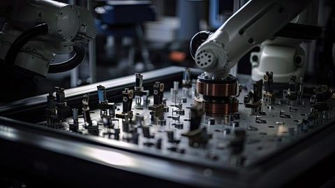
Wafer bonding equipment ranges from compact laboratory systems to automated manufacturing platforms. Basic systems may support manual loading and controlled bonding, while more advanced systems incorporate robotic handling, automated alignment, process monitoring, and recipe management.
Important equipment components include wafer holders or chucks, alignment cameras, temperature-control units, pressure mechanisms, vacuum chambers, and control software. Depending on the bonding method, the machine may also contain an electrical field generator, heating elements, gas controls, or a system for dispensing and curing adhesive materials.
Importance
Wafer bonding machines matter because modern semiconductor devices increasingly combine multiple functional layers rather than relying entirely on a single flat chip. These layers may contain processing circuits, memory, sensors, optical components, or structures that interact mechanically. Bonding allows manufacturers to integrate these elements while managing physical dimensions and electrical or mechanical connections.
The technology affects consumer electronics, automotive electronics, telecommunications, medical instruments, industrial sensors, and scientific equipment. For example, image sensors use layered structures to support light detection and signal processing, while MEMS devices may require bonded cavities to protect moving microscopic parts.
Manufacturing Challenges Addressed by Wafer Bonding
Wafer bonding helps address several technical challenges:
Device integration: Combining separately manufactured layers or components into one assembly.
Miniaturization: Supporting compact structures and closely spaced connections.
Environmental protection: Enclosing sensitive structures within sealed cavities where the design requires it.
Material compatibility: Joining selected combinations of silicon, glass, metals, and other suitable materials.
Thermal management: Integrating structures that may need different thermal or electrical properties.
Production consistency: Controlling alignment, pressure, temperature, and bonding time across repeated manufacturing cycles.
Bonding does not eliminate every manufacturing challenge. Particles, surface defects, trapped gas, uneven pressure, material expansion, and misalignment can weaken a joint or reduce device yield. Manufacturers therefore use inspection and process monitoring to identify defects and maintain consistent production conditions.
Comparing Wafer Bonding Methods
| Bonding method | Main mechanism | Typical applications |
|---|---|---|
| Direct bonding | Close contact between prepared surfaces | Silicon integration and stacked wafers |
| Fusion bonding | Surface contact strengthened by heat | Silicon-based structures and optical devices |
| Anodic bonding | Heat and an electric field | Glass-silicon sensor packages |
| Adhesive bonding | Cured adhesive layer | MEMS packaging and dissimilar materials |
| Eutectic bonding | Temperature-controlled metal joining | Hermetic packages and device assemblies |
| Hybrid bonding | Dielectric joining with metal connections | Advanced chip stacking and 3D integration |
Actual process suitability depends on material combinations, surface preparation, device design, and manufacturing requirements.
Recent Updates
Developments in wafer bonding from 2024 through 2026 have been closely connected to advanced semiconductor packaging, three-dimensional integration, and the growing need to connect multiple chips within compact electronic systems. Progress varies across manufacturers and applications, but the general direction is toward finer interconnections, improved process control, and compatibility with increasingly complex device structures.
Hybrid Bonding and Advanced Packaging
Hybrid bonding has gained attention in advanced semiconductor manufacturing because it combines dielectric-to-dielectric bonding with direct metal-to-metal electrical connections. This approach can support closely spaced interconnects in stacked memory and other advanced chip assemblies.
As connection spacing becomes smaller, alignment and surface preparation become increasingly demanding. Wafer bonding equipment must control particle contamination, wafer flatness, surface condition, and positioning accuracy. The precise requirements depend on the device architecture and process design.
Automation and Process Monitoring
Modern wafer bonding platforms increasingly use automated wafer handling, optical alignment, recipe controls, and monitoring systems. These features help operators manage repeatable processing conditions and record manufacturing information.
Data analysis can also help identify patterns associated with defects, equipment drift, or inconsistent bonding conditions. Automated inspection does not remove the need for engineering review, and process results still depend on equipment calibration, material quality, and validated operating procedures.
New Materials and Three-Dimensional Integration
Research and development continue to explore bonding approaches for silicon, compound semiconductors, glass, and other functional materials. These combinations can support optical systems, radio-frequency devices, power electronics, sensors, and specialized computing structures.
Three-dimensional integration places functional layers or dies above one another rather than arranging every component side by side. Wafer bonding can support this architecture, although thermal expansion, mechanical stress, heat removal, and electrical performance remain important engineering considerations.
Laws or Policies
Wafer bonding machines are influenced by semiconductor manufacturing standards, workplace safety rules, environmental requirements, and export-control regulations. The applicable requirements depend on the equipment's technical capabilities, the materials used, the destination market, and the facility in which manufacturing takes place.
Semiconductor Equipment Rules in India
In India, semiconductor manufacturing facilities must comply with relevant national and state requirements covering industrial operations, electrical safety, worker protection, building and fire safety, and environmental management. Requirements may apply to chemical handling, exhaust systems, hazardous materials, waste disposal, and equipment installation.
Government initiatives supporting semiconductor and electronics manufacturing provide a broader policy context. India's semiconductor and display manufacturing programmes have been intended to strengthen domestic capabilities, encourage investment, and develop manufacturing infrastructure. Eligibility and implementation conditions depend on the applicable programme guidelines.
International Standards and Export Controls
International standards may address equipment safety, electrical systems, contamination control, risk management, and semiconductor manufacturing processes. The relevance of a particular standard depends on the machine design, intended use, and requirements of the customer or facility.
Some semiconductor manufacturing equipment and related technology may be subject to export controls, particularly when it falls within specified technical categories or is transferred to restricted destinations or end users. Requirements vary by jurisdiction. Businesses involved in international equipment transfers must determine which rules apply to the specific machine and transaction.
These regulatory considerations do not mean that every wafer bonding machine is subject to the same restrictions. Technical specifications, destination, intended use, and current regulations determine the applicable obligations.
Tools and Resources
Several technical resources help engineers, researchers, and manufacturing teams understand wafer bonding equipment and evaluate process requirements. Their usefulness depends on whether the task involves early research, laboratory experimentation, equipment selection, or production monitoring.
Equipment and Process Resources
Manufacturer technical documentation commonly describes wafer dimensions, alignment capabilities, temperature ranges, pressure controls, vacuum performance, substrate compatibility, and automation options. Process notes and application documents can explain how different bonding methods behave under specific conditions.
Research papers and semiconductor engineering publications provide information about surface preparation, bond strength, void formation, hybrid bonding, and three-dimensional integration. Technical details should be evaluated in the context of the materials and process conditions studied.
Measurement and Inspection Tools
Common tools used around wafer bonding include:
Optical alignment systems: Measure and correct the relative position of wafers or dies.
Surface inspection equipment: Identify particles, scratches, and other visible defects.
Bond inspection systems: Detect voids or interface defects using suitable imaging or acoustic techniques.
Temperature and pressure sensors: Monitor key process conditions during bonding.
Metrology instruments: Measure wafer thickness, flatness, surface roughness, and dimensional variation.
Process data systems: Record equipment settings, inspection results, and production history.
No single inspection method detects every defect. A combination of measurements may be necessary to assess bond integrity and determine whether a process meets the intended specifications.
Research and Standards Platforms
Technical information is available through semiconductor research publications, the IEEE Xplore Digital Library, the SEMI industry association, and the websites of equipment manufacturers. Government sources such as India's Ministry of Electronics and Information Technology provide information about semiconductor policy and manufacturing initiatives.
When comparing technical documents, it is important to distinguish laboratory results from production-scale performance. Reported capabilities may depend on substrate size, surface preparation, process configuration, and inspection criteria.
FAQs
What is a wafer bonding machine used for?
A wafer bonding machine joins semiconductor wafers or other compatible substrates to create integrated structures. Applications include MEMS devices, image sensors, advanced chip packaging, optical components, and sealed semiconductor assemblies.
What are the main wafer bonding methods?
Common methods include direct bonding, fusion bonding, anodic bonding, adhesive bonding, eutectic bonding, and hybrid bonding. Each method uses different physical or chemical mechanisms and has specific material and process requirements.
How does hybrid wafer bonding work?
Hybrid wafer bonding joins prepared dielectric surfaces while forming metal-to-metal electrical connections between aligned structures. It supports dense interconnections in applications such as advanced chip stacking, where alignment and surface cleanliness are critical.
Which factors affect wafer bonding machine selection?
Important factors include wafer size, substrate materials, bonding method, alignment accuracy, temperature range, pressure control, vacuum capability, throughput requirements, and inspection options. The intended semiconductor application determines which specifications matter most.
What defects can occur during wafer bonding?
Potential defects include voids, particles trapped at the interface, weak bonds, misalignment, surface damage, and stress caused by differences in material expansion. Surface preparation, controlled processing, and suitable inspection methods help manufacturers identify and manage these issues.
Conclusion
Wafer bonding machines join compatible substrates to support semiconductor integration, microscopic device packaging, and three-dimensional chip structures. Direct, fusion, anodic, adhesive, eutectic, and hybrid bonding methods address different material combinations and manufacturing requirements. Recent developments emphasize finer interconnections, automation, and improved process monitoring. Equipment capabilities, applicable regulations, and inspection requirements vary according to the application and manufacturing environment.