Semiconductor Lithography Equipment Guide: EUV, DUV, Wafer Patterning and Manufacturing Processes
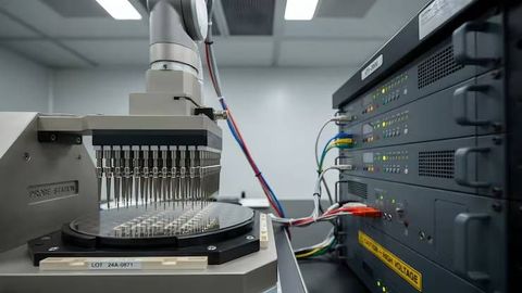
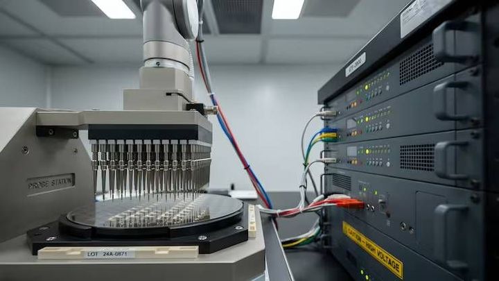
Semiconductor lithography equipment is used to transfer intricate circuit patterns onto silicon wafers during chip manufacturing. A semiconductor lithography equipment guide explains technologies such as extreme ultraviolet (EUV) lithography, deep ultraviolet (DUV) lithography, wafer patterning, and the processes that turn circuit designs into physical structures. These technologies are essential for producing the processors, memory chips, sensors, and control components found in computers, smartphones, vehicles, and industrial machinery.
Context
Semiconductor lithography equipment is used to transfer intricate circuit patterns onto silicon wafers during chip manufacturing. A semiconductor lithography equipment guide explains technologies such as extreme ultraviolet (EUV) lithography, deep ultraviolet (DUV) lithography, wafer patterning, and the processes that turn circuit designs into physical structures. These technologies are essential for producing the processors, memory chips, sensors, and control components found in computers, smartphones, vehicles, and industrial machinery.
The development of lithography began with techniques adapted from photography and printing. As semiconductor devices became smaller and more complex, manufacturers needed methods to reproduce increasingly fine patterns across large numbers of microscopic components. Modern lithography systems combine specialized light sources, precision optics, wafer-handling mechanisms, and computer-controlled alignment systems to achieve this task.
How Semiconductor Lithography Works
Lithography generally begins with a silicon wafer coated with a light-sensitive material called photoresist. A patterned mask or reticle, or a pattern generated through a maskless method in certain applications, defines which areas of the photoresist are exposed to light. The exposed or unexposed regions respond differently during development, creating a temporary pattern on the wafer.
This pattern guides subsequent manufacturing operations, including etching, material deposition, or ion implantation. Repeating these steps creates the multiple layers required for an integrated circuit. Lithography is therefore one part of a broader manufacturing sequence rather than a process that produces a complete chip by itself.
Main Types of Lithography Equipment
Two major optical approaches used in advanced chip manufacturing are EUV and DUV lithography. They differ mainly in the wavelength of light they use, the patterns they can resolve under particular conditions, and the complexity of the equipment involved.
EUV lithography: Uses extreme ultraviolet light with a wavelength of approximately 13.5 nanometers. It is used for selected fine-patterning layers in advanced logic and other semiconductor manufacturing processes.
DUV lithography: Uses deep ultraviolet light, commonly at wavelengths of 248 nm or 193 nm in major semiconductor applications. It remains important for many logic, memory, analog, and power semiconductor processes.
Immersion lithography: A form of 193 nm DUV lithography that places a liquid, usually purified water, between the final projection lens and the wafer to improve optical resolution.
Maskless lithography: Uses controlled beams, such as electron beams, to write patterns directly without a conventional optical mask. It is used in applications such as research, prototyping, and specialized manufacturing.
The appropriate method depends on the required feature dimensions, device design, production volume, process complexity, and manufacturing equipment available.
Importance
Semiconductor lithography equipment matters because the dimensions and accuracy of circuit patterns influence how electronic devices perform. Transistors, wiring structures, and other components must be formed in precisely controlled locations across the wafer. Small patterning errors can affect electrical behavior, manufacturing yield, and the reliability of the finished chip.
The technology also affects industries beyond semiconductor manufacturing. Automotive electronics, cloud computing, telecommunications, medical equipment, renewable energy systems, and factory automation all rely on chips produced through multiple semiconductor fabrication processes. Different applications require different chip designs, so not every device depends on the most advanced lithography technology.
Wafer Patterning and Manufacturing Challenges
Wafer patterning involves several connected stages, each of which must be controlled carefully. Common challenges include:
Resolution: Reproducing small circuit features with sufficient detail.
Overlay accuracy: Aligning a new pattern with structures formed in earlier layers.
Defect control: Preventing particles, resist defects, and pattern irregularities from affecting the wafer.
Process stability: Maintaining consistent exposure, focus, temperature, and wafer positioning.
Production throughput: Processing wafers at a practical rate without compromising required pattern quality.
These challenges are interconnected. Increasing resolution alone does not ensure successful manufacturing because the resulting pattern must also align with previous layers and remain consistent across the wafer.
Comparing EUV and DUV Lithography
| Feature | EUV lithography | DUV lithography |
|---|---|---|
| Typical wavelength | 13.5 nm | 193 nm or 248 nm |
| Light source | Specialized EUV source | Excimer laser sources |
| Optical system | Reflective optics | Primarily refractive optics, depending on system |
| Common role | Selected fine-patterning layers | Wide range of semiconductor layers and devices |
| Patterning approach | Can reduce the need for some multiple-patterning steps | May use multiple-patterning techniques for very fine features |
| Equipment complexity | Requires vacuum operation and specialized reflective optics | Depends on system type; established infrastructure is widely used |
EUV and DUV are complementary technologies rather than direct substitutes in every situation. A single advanced chip may use EUV for some layers and DUV for others, depending on the manufacturing process.
Recent Updates
Developments in semiconductor lithography from 2024 through 2026 have centered on finer patterning, equipment productivity, process control, and the expansion of semiconductor manufacturing capacity. The pace of deployment differs across manufacturers and regions, and announced technical capabilities do not necessarily mean that every facility has adopted them for high-volume production.
High-NA EUV and Advanced Patterning
High numerical aperture (High-NA) EUV lithography is a major development intended to improve optical resolution. By using a projection system with a higher numerical aperture, these systems can print smaller features under suitable process conditions. Their adoption requires changes to equipment integration, masks, photoresists, wafer handling, and manufacturing procedures.
High-NA EUV also introduces practical challenges, including equipment complexity, process qualification, and the need to control defects. Manufacturers must determine how the technology fits into particular chip designs and production flows rather than assuming that every layer will use it.
DUV Improvements and Process Integration
DUV lithography continues to evolve through improvements in alignment, exposure control, computational lithography, and multi-patterning techniques. Multi-patterning divides a complex layout into several exposures or pattern-transfer stages to produce features that may be difficult to create in a single exposure.
Software-based techniques also help compensate for optical effects and expected manufacturing variation. These methods support the creation of accurate patterns, although they can add steps and increase the importance of process coordination.
Automation and Equipment Monitoring
Modern lithography systems use sensors, automated wafer handling, equipment diagnostics, and advanced control software. Manufacturing facilities analyze process data to identify changes in exposure conditions, alignment, or equipment behavior. These systems can support process consistency, but their effectiveness depends on calibration, data quality, and integration with the wider fabrication process.
Laws or Policies
Semiconductor lithography equipment is affected by national manufacturing policies, export controls, intellectual property rules, workplace safety requirements, and environmental regulations. The exact requirements depend on the equipment, its specifications, the parties involved, and the destination country.
Semiconductor Policy and Export Controls
In the United States, semiconductor manufacturing equipment and related technologies may be subject to export controls administered by the Bureau of Industry and Security. Certain advanced equipment, software, technology, and transactions involving specific destinations or end users may require authorization or face restrictions. The applicable rules depend on the item classification and the circumstances of the transaction.
Other jurisdictions also maintain trade-control frameworks, and requirements can change as technology and international policy evolve. Manufacturers and research institutions must assess applicable regulations rather than assuming that all lithography equipment can be transferred internationally without restrictions.
Manufacturing Programs in India
India has introduced semiconductor development initiatives, including the India Semiconductor Mission and the Semicon India Programme, to encourage domestic semiconductor and display manufacturing capabilities. Support arrangements, eligibility criteria, and approved projects are governed by the relevant programme guidelines and government decisions.
Semiconductor facilities must also comply with applicable Indian requirements concerning factory operations, electrical safety, environmental permissions, hazardous materials, and worker protection. The precise obligations depend on the facility, the chemicals and processes used, and the relevant national and state rules.
Environmental and Workplace Requirements
Lithography and related wafer-processing operations may involve photoresists, solvents, specialty gases, and other controlled materials. Facilities therefore need suitable chemical handling, ventilation, waste management, emergency procedures, and worker training. EUV systems also require specialized vacuum and radiation-control engineering appropriate to their operating conditions.
Tools and Resources
Technical resources help readers understand lithography equipment, compare process technologies, and follow developments in semiconductor manufacturing. Different resources serve different purposes, from basic explanations to detailed technical specifications.
Technical Documentation and Industry Resources
ASML: Publishes technical explanations of EUV, DUV, lithography principles, and semiconductor manufacturing equipment.
SEMI: Provides semiconductor industry standards, technical information, and manufacturing-related resources.
IEEE: Publishes research and engineering material covering lithography, microelectronics, device fabrication, and process development.
imec: Shares research on advanced semiconductor processing, patterning, and emerging lithography techniques.
U.S. Bureau of Industry and Security: Provides official information about applicable export-control regulations and licensing requirements.
Equipment manufacturers' technical documentation can explain system architecture, light sources, optical components, and wafer-handling capabilities. Public summaries may not include every specification, operating limitation, or process requirement.
Process Design and Research Tools
Computational lithography software supports optical proximity correction, mask optimization, and simulation of pattern formation. Electronic design automation tools help engineers develop circuit layouts, while process simulation tools can examine selected manufacturing behaviors.
Research laboratories may also use scanning electron microscopes, critical-dimension measurement systems, overlay metrology, and defect-inspection equipment to examine patterns after exposure and processing. These tools provide different measurements and are generally used together to assess whether a wafer meets the requirements of a particular process.
FAQs
What is semiconductor lithography equipment used for?
Semiconductor lithography equipment transfers circuit patterns onto photoresist-coated wafers. These patterns guide later manufacturing steps that form transistors, wiring, and other structures inside integrated circuits.
What is the difference between EUV and DUV lithography?
EUV lithography uses light at approximately 13.5 nm, while common DUV systems use wavelengths such as 193 nm and 248 nm. EUV supports selected fine-patterning layers, whereas DUV remains widely used across many semiconductor processes.
How does wafer patterning work in semiconductor manufacturing?
Wafer patterning generally involves coating a wafer with photoresist, exposing it to a defined pattern, developing the resist, and transferring the resulting pattern through processes such as etching. The sequence is repeated to create multiple device layers.
What is High-NA EUV lithography?
High-NA EUV is an advanced lithography approach that uses a higher numerical aperture in the projection optics to improve resolution. Its use requires specialized equipment and process adjustments, and adoption depends on manufacturing requirements.
Which tools are used to inspect semiconductor lithography patterns?
Common tools include scanning electron microscopes, critical-dimension metrology systems, overlay measurement equipment, and defect-inspection systems. Each evaluates different aspects of pattern size, alignment, or manufacturing quality.
Conclusion
Semiconductor lithography equipment enables the precise patterning required to manufacture modern integrated circuits. EUV and DUV technologies support different manufacturing needs, while wafer patterning depends on careful control of exposure, alignment, defects, and subsequent process steps. Developments such as High-NA EUV, computational lithography, and automated monitoring continue to shape the field. Trade controls, manufacturing policies, and workplace regulations also influence how lithography equipment is developed, transferred, and operated.