Semiconductor Wafer Bonding Machines Guide: Technologies, Materials, Methods and Industrial Uses
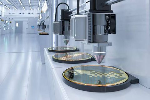
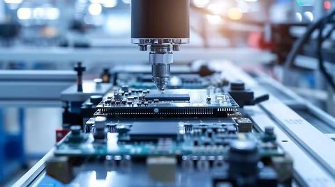
Semiconductor wafer bonding machines are specialized systems used to join two or more semiconductor wafers or wafer-like substrates into a single structure. These machines play an important role in semiconductor manufacturing, microelectromechanical systems (MEMS), advanced packaging, optical devices, and sensor production.
Context
Semiconductor wafer bonding machines are specialized systems used to join two or more semiconductor wafers or wafer-like substrates into a single structure. These machines play an important role in semiconductor manufacturing, microelectromechanical systems (MEMS), advanced packaging, optical devices, and sensor production. Wafer bonding developed as semiconductor applications required increasingly complex structures that could not always be produced through conventional processes on a single wafer.
A semiconductor wafer is a thin, flat disc made from materials such as silicon, glass, or other engineered substrates. Individual wafers contain or support microscopic electronic structures. Wafer bonding connects separate layers to create devices with particular electrical, mechanical, thermal, or optical characteristics.
Understanding Semiconductor Wafer Bonding Machines
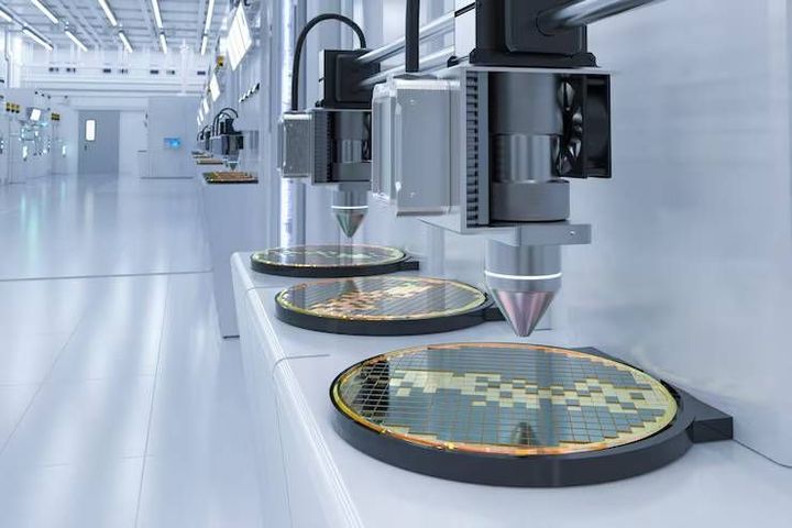
A wafer bonding machine applies controlled pressure, temperature, surface contact, or other forms of energy to join wafer surfaces. The process depends on the materials involved and the intended device structure. Some bonding methods require high temperatures, while others operate at lower temperatures to protect delicate electronic components.
A typical wafer bonding process involves several stages:
Surface preparation: Removing particles, residues, and unwanted surface layers.
Alignment: Positioning wafers according to the required pattern or device layout.
Contact and bonding: Bringing the surfaces together under specified conditions.
Bond strengthening: Applying heat, pressure, or another treatment when required.
Inspection: Checking alignment, bond strength, voids, and structural quality.
The equipment may be used in research laboratories, pilot production facilities, or semiconductor manufacturing plants. Machine configuration depends on wafer diameter, substrate materials, production volume, and process requirements.
Importance
Semiconductor wafer bonding matters because modern electronic devices often require several materials or functional layers to work together. A single silicon wafer may not provide every electrical, optical, mechanical, or thermal property required for a particular application. Bonding allows manufacturers to combine different layers into compact structures.
The process supports technologies used in smartphones, automotive electronics, medical instruments, optical communication equipment, industrial sensors, and computing hardware. For example, MEMS devices may combine mechanical structures with electronic circuits, while advanced semiconductor packaging can connect separately manufactured components into a more integrated assembly.
Industrial Applications of Wafer Bonding
Different industries use wafer bonding to address specific manufacturing requirements.
Advanced semiconductor packaging: Joining dies or wafers to support compact electronic assemblies and vertical interconnections.
MEMS manufacturing: Combining silicon structures with glass or other materials to create sensors, accelerometers, and pressure-measurement devices.
Power electronics: Integrating materials and structures that help manage electrical and thermal requirements.
Optoelectronics: Joining substrates used in optical sensors, photonic components, and light-based communication systems.
Microfluidics: Creating enclosed channels and chambers for laboratory instruments and analytical devices.
Research and development: Testing new substrate combinations, bonding techniques, and device architectures.
Bonding quality can affect electrical performance, heat transfer, structural reliability, and device yield. Surface contamination, trapped air, uneven pressure, or incorrect alignment may produce defects that are difficult to correct after bonding.
Common Wafer Bonding Technologies
Several technologies are used in semiconductor wafer bonding. Each has different operating requirements and material limitations.
| Bonding technology | Basic principle | Common applications |
|---|---|---|
| Direct bonding | Prepared surfaces join through close contact and interfacial forces | Silicon structures, wafer stacking |
| Fusion bonding | Surfaces bond through contact followed by heat treatment | Silicon and selected insulating substrates |
| Anodic bonding | An electric field and heat join suitable glass and silicon combinations | MEMS devices, sealed sensor structures |
| Adhesive bonding | An intermediate polymer or adhesive layer joins substrates | Optical devices, packaging, temperature-sensitive structures |
| Thermocompression bonding | Heat and pressure create a bond between suitable surfaces | Metal interconnections, advanced packaging |
| Hybrid bonding | Dielectric bonding and conductive connections form together | High-density chip integration |
The suitability of a method depends on surface condition, material compatibility, alignment accuracy, temperature limits, and the electrical or mechanical properties required in the finished device.
Recent Updates
From 2024 through 2026, semiconductor manufacturing has continued to place greater emphasis on advanced packaging, heterogeneous integration, and three-dimensional chip architectures. These approaches combine components or materials that may be manufactured separately, creating a need for precise wafer and die bonding processes.
Advanced Packaging and Hybrid Bonding
Hybrid bonding has received growing attention because it can combine dielectric surfaces with fine-pitch electrical connections. Compared with conventional interconnection approaches, it can support closer spacing between connections when the materials, surface preparation, and process controls are suitable.
This technology is relevant to stacked memory, logic integration, image sensors, and other high-density electronic assemblies. However, successful implementation requires careful control of surface flatness, cleanliness, alignment, and bonding conditions. Small particles or dimensional errors can affect a large number of closely spaced connections.
Low-Temperature and Material Integration
Low-temperature wafer bonding is also important when processing temperature-sensitive components or combining materials with different thermal expansion characteristics. Researchers and manufacturers continue to examine surface activation, plasma-assisted preparation, adhesive layers, and other techniques that can support bonding under particular process conditions.
Automation and inspection technologies are also developing. Machine-control systems can monitor pressure, temperature, alignment, and process timing, while inspection equipment can help identify voids and surface defects. These capabilities support process consistency, although results depend on equipment design and manufacturing controls.
Laws or Policies
Semiconductor wafer bonding machines are affected by industrial safety rules, environmental requirements, product standards, and regulations governing semiconductor equipment and materials. The exact requirements depend on the country where the equipment is installed, the substances used, and the manufacturing activities being performed.
Industrial Safety and Environmental Requirements in India
In India, semiconductor manufacturing facilities may be subject to applicable occupational safety, factory, electrical safety, environmental, and fire protection requirements. The relevant obligations depend on the facility, the applicable state rules, and the legal framework in force.
Wafer bonding equipment may involve heated surfaces, high-pressure mechanisms, electrical systems, vacuum chambers, or process gases. Appropriate machine guarding, emergency controls, ventilation, maintenance procedures, and operator training are therefore important parts of safe operation.
Facilities handling chemicals or generating regulated waste may also need to follow applicable environmental and hazardous-waste requirements. Equipment installation and operation should account for the specific hazards associated with the selected process.
Semiconductor Manufacturing Initiatives and Standards
India's semiconductor development programs, including the India Semiconductor Mission, support the broader development of semiconductor manufacturing and related technologies. Specific eligibility conditions and program requirements depend on the applicable scheme and its current provisions.
International standards may also guide equipment design, contamination control, electrical safety, and semiconductor manufacturing practices. The SEMI standards program develops technical standards relevant to semiconductor manufacturing equipment and materials. Standards may be voluntary or incorporated into contractual, regulatory, or facility requirements, depending on the circumstances.
Export controls can apply to certain semiconductor manufacturing equipment, technologies, and technical information. Requirements depend on the equipment's capabilities, destination, end user, and applicable national rules.
Tools and Resources
Technical resources help engineers, researchers, and manufacturing teams understand wafer bonding processes, evaluate machine capabilities, and monitor production quality.
Process Monitoring and Inspection Tools
Common tools used alongside wafer bonding machines include:
Optical alignment systems: Position wafers or dies relative to reference marks.
Surface inspection equipment: Detect particles, scratches, and surface irregularities.
Infrared inspection: Examine selected bonded structures for internal voids or interface defects when materials and equipment permit.
Acoustic microscopy: Identify certain internal defects through reflected sound waves.
Bond-strength testing equipment: Measure mechanical separation or adhesion characteristics using an appropriate test method.
Temperature and pressure monitoring: Record process conditions during bonding.
No single inspection technique identifies every defect. Manufacturers often combine several methods based on wafer materials, device structure, production requirements, and the limits of each instrument.
Technical Information and Planning Resources
The SEMI website provides information about semiconductor industry standards and manufacturing practices. The IEEE Xplore digital library contains technical papers on wafer bonding, semiconductor packaging, and device integration. Research institutions and semiconductor equipment manufacturers may also publish application notes explaining specific bonding methods.
Process planning templates can record substrate material, wafer diameter, surface preparation, alignment tolerance, bonding temperature, applied pressure, process duration, and inspection results. Keeping these details together helps teams compare experimental runs and investigate process variation.
FAQs
What is a semiconductor wafer bonding machine?
A semiconductor wafer bonding machine joins two or more wafers or substrates under controlled conditions. It is used to create layered structures for semiconductor devices, sensors, optical components, and advanced packaging.
What are the main types of wafer bonding technologies?
Common types include direct bonding, fusion bonding, anodic bonding, adhesive bonding, thermocompression bonding, and hybrid bonding. Each method has different requirements for materials, surface preparation, temperature, and pressure.
What materials are used in semiconductor wafer bonding?
Materials may include silicon, glass, silicon dioxide, selected compound semiconductors, metals, and bonding polymers. Compatibility depends on the intended device, surface properties, thermal behavior, and bonding method.
Why is hybrid bonding important in semiconductor manufacturing?
Hybrid bonding combines dielectric bonding with conductive electrical connections. It can support dense interconnections in stacked chips and advanced packaging when alignment, surface quality, and process conditions meet the required specifications.
How is wafer bonding quality inspected?
Inspection may include optical alignment checks, surface analysis, infrared imaging, acoustic microscopy, and mechanical bond-strength tests. The appropriate method depends on the substrate materials and the type of defect being investigated.
Conclusion
Semiconductor wafer bonding machines join materials and device layers for applications ranging from MEMS sensors to advanced chip packaging. Different bonding technologies address different requirements for surface preparation, temperature, pressure, electrical connections, and material compatibility. Recent developments in hybrid bonding and three-dimensional integration have increased the importance of precise process control and defect inspection. Industrial safety rules, environmental requirements, technical standards, and export controls may also affect equipment use and manufacturing operations.