Modern Wafer Process Information With Semiconductor Manufacturing, Inspection, and Process Optimization
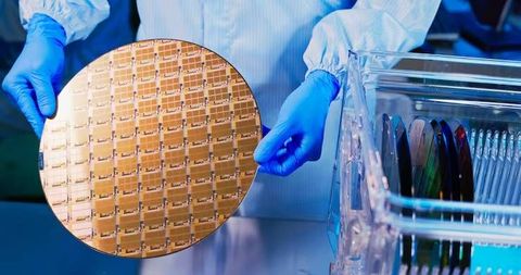
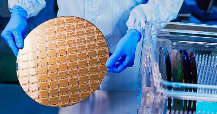
Modern wafer process information describes the methods, measurements, equipment, and data used to transform semiconductor wafers into precisely patterned electronic structures. A wafer is a thin, usually circular piece of semiconductor material that provides the foundation for manufacturing integrated circuits.
The process involves multiple stages, including wafer preparation, thin-film deposition, photolithography, etching, cleaning, doping, inspection, measurement, and packaging preparation.
Semiconductor manufacturing depends on extremely controlled conditions because electronic components are created at very small dimensions. A minor variation in film thickness, temperature, chemical concentration, alignment, or surface condition can affect the performance of a finished device. For this reason, wafer processing combines materials science, mechanical engineering, chemistry, electronics, software, and data analysis.
Modern wafer process information is also connected with process optimization. Manufacturers collect measurements throughout production and use them to understand variation, identify process problems, and maintain consistent results. Inspection systems examine wafer surfaces and patterns, while metrology equipment measures physical characteristics such as thickness, dimensions, roughness, and alignment.
From Silicon Material to Processed Wafer
The manufacturing journey begins with semiconductor material that is formed into a highly controlled wafer. The wafer surface is polished and prepared before entering a sequence of fabrication processes.
Important stages commonly include:
- Wafer preparation, which establishes a clean and controlled surface.
- Deposition, which places thin layers of material onto the wafer.
- Photolithography, which transfers selected patterns onto a photo-sensitive layer.
- Etching, which removes specific areas of material.
- Doping, which changes selected electrical properties of the semiconductor.
- Cleaning, which removes unwanted particles and chemical residues.
- Inspection and metrology, which measure defects and process characteristics.
These stages may be repeated many times to construct increasingly complex structures. Modern semiconductor manufacturing therefore relies on process information collected throughout the entire production sequence.
Role of Wafer Inspection
Wafer inspection is used to identify defects, contamination, pattern abnormalities, and other conditions that can affect manufacturing results. Optical inspection can examine wafer surfaces using light, while other inspection approaches can detect characteristics that are difficult to identify through conventional visual methods.
Inspection data can be connected with manufacturing process data to identify relationships between equipment settings and wafer results. This creates a feedback system in which measurements help engineers understand whether a process remains within defined operating limits.
Importance
Modern wafer process information matters because semiconductors are incorporated into computers, communication equipment, vehicles, industrial systems, medical devices, consumer electronics, and many other technologies. As electronic systems become more complex, semiconductor manufacturing requires greater control over materials, dimensions, contamination, and process variation.
The topic affects several groups. Engineers use wafer process information to analyze production conditions, equipment teams use it to understand machine behavior, quality teams examine defect patterns, and researchers study new materials and manufacturing techniques. Consumers may not interact directly with wafer processing, but the reliability and performance of many electronic products depend on these manufacturing processes.
Managing Process Variation
One of the central challenges in semiconductor manufacturing is process variation. Manufacturing equipment operates under controlled conditions, but small differences can still occur because of temperature changes, material properties, equipment wear, chemical conditions, or environmental factors.
Process optimization attempts to identify and reduce these variations. Statistical process control, process capability analysis, sensor monitoring, and historical production data can help identify unusual patterns before they become larger manufacturing problems.
A simplified example is shown below:
| Process Area | Typical Information Collected | Purpose |
|---|---|---|
| Wafer preparation | Surface condition, particles | Surface quality control |
| Deposition | Film thickness, uniformity | Layer consistency |
| Lithography | Pattern dimensions, alignment | Pattern accuracy |
| Etching | Etch depth, profile | Structure formation |
| Cleaning | Particle levels, residue | Contamination control |
| Inspection | Defect location and type | Defect identification |
| Metrology | Dimensions and material properties | Process measurement |
Importance of Data Integration
Modern semiconductor manufacturing generates large quantities of process information. A single wafer can pass through numerous process steps, with each stage producing measurements and equipment records.
Data integration allows information from different stages to be examined together. For example, a defect detected during inspection can potentially be compared with deposition conditions, lithography measurements, etching parameters, or equipment sensor readings from earlier stages.
This approach supports root-cause analysis and helps distinguish isolated defects from systematic process patterns. It also provides a foundation for statistical models and machine-learning systems used for process monitoring.
Recent Updates
From 2024 through 2026, semiconductor manufacturing has continued moving toward more advanced process control, automated inspection, data integration, and increasingly complex device structures. The expansion of artificial intelligence hardware has increased attention on semiconductor manufacturing capacity and the technologies required to produce high-density electronic components.
Advanced Process Control
Advanced process control increasingly combines equipment sensors, metrology results, historical process data, and statistical models. Instead of examining each measurement separately, manufacturers can evaluate multiple variables together to identify relationships and unusual behavior.
Machine-learning techniques are also being explored for defect classification, equipment monitoring, predictive analysis, and process optimization. These systems generally work alongside established engineering controls rather than replacing physical measurement and inspection.
Smaller Features and Complex Structures
Modern semiconductor devices can contain extremely small structures and multiple layers of materials. Newer manufacturing approaches also involve three-dimensional structures and advanced packaging configurations.
As structures become more complex, wafer inspection and metrology must identify increasingly subtle differences. This has encouraged development of higher-resolution measurement systems, improved image analysis, and more automated defect classification.
Manufacturing Data and Digital Systems
Manufacturing facilities are also placing greater emphasis on connecting equipment, sensors, process databases, and analytical platforms. Digital manufacturing systems can organize information from different stages and make it easier to identify process trends.
Digital twins and simulation environments are being explored for equipment analysis and process planning. These approaches can model manufacturing behavior using physical and historical information, although the usefulness of a model depends on data quality and appropriate validation.
Laws or Policies
Semiconductor manufacturing is influenced by a combination of environmental, workplace, chemical handling, equipment safety, data management, and trade-related requirements. Exact rules differ by country and manufacturing location, so organizations generally need to follow the regulatory framework applicable to their facilities.
Environmental and Chemical Controls
Wafer fabrication can involve specialized chemicals, gases, solvents, and materials. Facilities therefore operate under rules concerning chemical storage, handling, emissions, waste management, water use, and environmental protection.
Manufacturing facilities may also need systems for monitoring emissions and managing industrial waste. Requirements vary according to the materials used and the jurisdiction where production takes place.
Workplace and Equipment Safety
Semiconductor manufacturing equipment can involve high temperatures, vacuum systems, electrical energy, pressurized gases, chemicals, and moving components. Workplace safety frameworks commonly address exposure controls, equipment protection, emergency procedures, training, and facility management.
International technical standards can also influence equipment design, semiconductor manufacturing practices, measurement systems, and quality management. These standards help establish consistent technical procedures, although applicable requirements depend on the specific operation.
Government Semiconductor Programs
Governments in several regions have introduced programs intended to strengthen domestic semiconductor research, manufacturing capacity, workforce development, and supply-chain resilience. Such programs can influence investments in fabrication facilities, research centers, advanced packaging, and semiconductor equipment.
The specific eligibility requirements, funding structures, and policy conditions vary by jurisdiction and can change over time.
Tools and Resources
Modern wafer process information depends on a combination of physical equipment and digital analytical tools. Different facilities use different combinations according to their manufacturing processes.
Inspection and Metrology Equipment
Common equipment categories include optical inspection systems, critical-dimension measurement systems, film-thickness measurement tools, surface analysis instruments, particle monitoring equipment, and defect review systems.
These tools generate measurements that can be compared with predefined process limits. When measurements show unusual behavior, engineers can investigate the associated manufacturing stage.
Process Control Software
Manufacturing execution systems can organize production information and track wafers through multiple process stages. Statistical process control platforms can analyze measurements and identify changes in process behavior.
Data visualization platforms are also used to display trends, equipment measurements, defect distributions, and production information. These systems can make large datasets easier to interpret.
Simulation and Analytical Resources
Process simulation tools can model aspects of semiconductor fabrication before or during manufacturing. Statistical software can be used for experimental design, regression analysis, process capability studies, and variation analysis.
Machine-learning platforms may also be used for defect classification, anomaly detection, equipment monitoring, and predictive process analysis. Their results need to be evaluated against actual manufacturing measurements.
FAQs
What is modern wafer process information?
Modern wafer process information includes measurements, process parameters, inspection results, equipment data, and analytical information collected during semiconductor wafer manufacturing. It helps explain how manufacturing conditions affect wafer quality and process consistency.
How does wafer inspection work?
Wafer inspection uses optical, electrical, imaging, or other measurement techniques to identify defects and abnormalities. Inspection results can show where defects occur and help engineers investigate possible relationships with manufacturing conditions.
What is semiconductor manufacturing process optimization?
Semiconductor manufacturing process optimization involves analyzing process measurements and equipment conditions to reduce unwanted variation and maintain controlled manufacturing results. Statistical analysis, metrology, sensors, and automated systems can contribute to this work.
Why is wafer metrology important?
Wafer metrology provides quantitative measurements of characteristics such as film thickness, pattern dimensions, surface properties, and alignment. These measurements help determine whether a process is producing structures within defined specifications.
How is artificial intelligence used in wafer processing?
Artificial intelligence and machine-learning methods can analyze manufacturing datasets for defect classification, anomaly detection, equipment monitoring, and process analysis. These methods depend on suitable data and validation against physical manufacturing results.
Conclusion
Modern wafer process information connects semiconductor materials, fabrication equipment, inspection systems, metrology, and manufacturing data. Semiconductor manufacturing increasingly depends on precise measurement and process optimization as device structures become more complex. Recent developments have emphasized automated inspection, advanced process control, data integration, and analytical methods. Environmental, safety, and manufacturing requirements also shape how wafer fabrication facilities operate.