Explore Semiconductor Equipment Manufacturing: Guide to Lithography, Etching, and Fabrication Systems
Semiconductor equipment manufacturing is a critical part of the modern electronics ecosystem. It involves the design and production of advanced machines used to create semiconductor chips, which power everyday devices such as smartphones, computers, vehicles, and medical equipment. These machines operate in highly controlled environments and use precise processes to build microscopic circuits on silicon wafers.
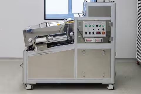
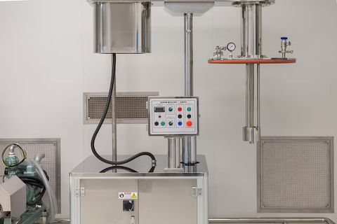
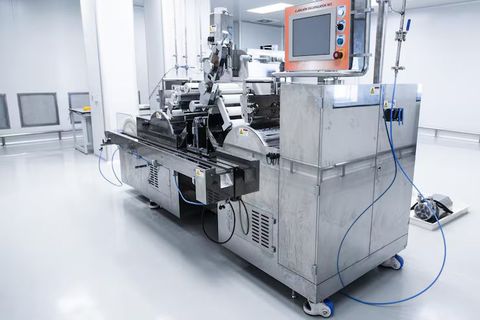
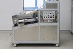
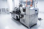
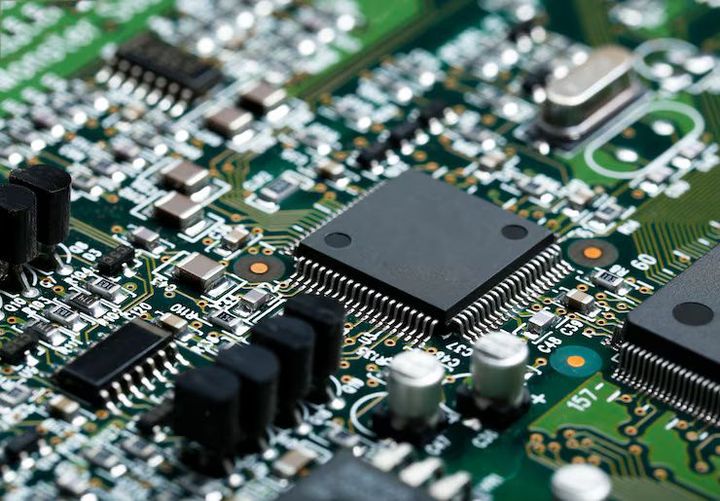
Three core processes define how semiconductor devices are made: lithography, etching, and fabrication systems. Lithography is used to transfer circuit patterns onto wafers, etching removes material to shape those patterns, and fabrication systems combine multiple steps to complete chip production. Together, these processes form the backbone of semiconductor equipment manufacturing and enable the creation of increasingly compact and efficient electronic components.
The origins of semiconductor manufacturing trace back to early research in solid-state physics. Over time, the demand for faster and smaller devices led to the development of specialized equipment capable of handling nanoscale operations. Today, this field continues to evolve as technology becomes more integrated into daily life.
Importance
Semiconductor equipment manufacturing plays a significant role in shaping modern infrastructure. It affects industries such as telecommunications, healthcare, transportation, and energy. Without reliable semiconductor fabrication systems, many technologies that people depend on would not function.
The importance of lithography and etching lies in their precision. As electronic devices become smaller, the circuits inside them must also shrink. This requires equipment that can operate at extremely fine scales. Even a small variation in these processes can impact the performance of a chip.
Several practical challenges highlight the importance of this field. These include maintaining clean manufacturing environments, managing energy consumption, and ensuring consistent production quality. Semiconductor equipment manufacturing addresses these challenges by developing advanced tools and techniques that improve accuracy and efficiency.
For everyday users, this translates into more reliable devices, improved battery life, and enhanced performance in applications such as communication and computing.
Recent Updates
Recent developments in semiconductor equipment manufacturing reflect ongoing efforts to meet growing global demand. Advances in lithography systems have enabled the production of smaller and more complex chip designs. Techniques such as extreme ultraviolet (EUV) lithography are being used to achieve finer pattern resolution.
Etching technology has also evolved to support new materials and structures. Modern etching tools can create three-dimensional patterns, which are essential for advanced chip architectures. This has contributed to improvements in memory and processing capabilities.
Fabrication systems are becoming more automated and interconnected. The use of artificial intelligence and data analytics helps monitor production processes and detect variations early. This reduces errors and enhances overall efficiency.
Another noticeable trend is the expansion of semiconductor manufacturing facilities in different regions. Governments and industries are investing in infrastructure to strengthen supply chains and reduce dependency on limited sources.
Laws or Policies
Semiconductor equipment manufacturing is influenced by a range of laws and policies that aim to regulate production, ensure safety, and support innovation. In many countries, governments provide guidelines for cleanroom standards, environmental impact, and worker safety.
Export regulations play an important role in this industry. Certain semiconductor equipment and technologies are subject to restrictions when transferred across borders. These policies are designed to manage the distribution of sensitive technologies.
Environmental policies also affect fabrication systems. Manufacturers are required to control emissions, manage chemical usage, and reduce waste generated during processes such as etching and lithography. Compliance with these regulations helps minimize environmental impact.
In addition, government initiatives often support research and development in semiconductor technology. These programs encourage collaboration between academic institutions and industry participants, helping to advance equipment design and manufacturing methods.
Tools and Resources
Understanding semiconductor equipment manufacturing involves access to various tools and resources that explain processes and technologies in simple terms. These resources can help learners, researchers, and industry observers explore the field more effectively.
Commonly used tools and resources include:
- Simulation software, which models lithography and etching processes to study how patterns are formed on wafers
- Educational platforms, which provide courses and tutorials on semiconductor fabrication systems
- Industry reports, which offer insights into trends and developments in semiconductor equipment manufacturing
- Technical standards documents, which outline guidelines for equipment performance and safety
A simplified comparison of core semiconductor processes is shown below:
| Process | Main Function | Key Equipment Used |
|---|---|---|
| Lithography | Transfers circuit patterns onto wafers | Photolithography systems |
| Etching | Removes material to define structures | Plasma etching equipment |
| Fabrication Systems | Integrates multiple steps in chip production | Integrated processing systems |
These tools and references provide a structured way to understand how semiconductor equipment operates and how different processes interact within fabrication systems.
FAQs
What is semiconductor equipment manufacturing?
Semiconductor equipment manufacturing refers to the production of machines used to create semiconductor chips. These machines perform processes such as lithography, etching, and fabrication systems to build electronic components.
How does lithography work in semiconductor manufacturing?
Lithography uses light to transfer circuit patterns onto a silicon wafer. A light-sensitive material is applied to the wafer, and specific patterns are projected onto it to define the structure of the chip.
What role does etching play in fabrication systems?
Etching removes unwanted material from the wafer after lithography. This process helps shape the circuit patterns and ensures that the design is accurately formed.
Why are fabrication systems important in chip production?
Fabrication systems combine multiple manufacturing steps into a coordinated process. They help maintain consistency and precision, which are essential for producing reliable semiconductor devices.
Are semiconductor manufacturing processes environmentally regulated?
Yes, semiconductor equipment manufacturing is subject to environmental regulations. These include guidelines for managing chemicals, reducing emissions, and handling waste generated during lithography and etching processes.
Conclusion
Semiconductor equipment manufacturing supports the development of modern electronic devices by enabling precise and efficient chip production. Processes such as lithography, etching, and fabrication systems work together to create complex circuits at very small scales. Advances in technology continue to improve these processes, while regulations help ensure safe and responsible manufacturing. As demand for electronics grows, this field remains essential to technological progress.